Soot from an electric arc
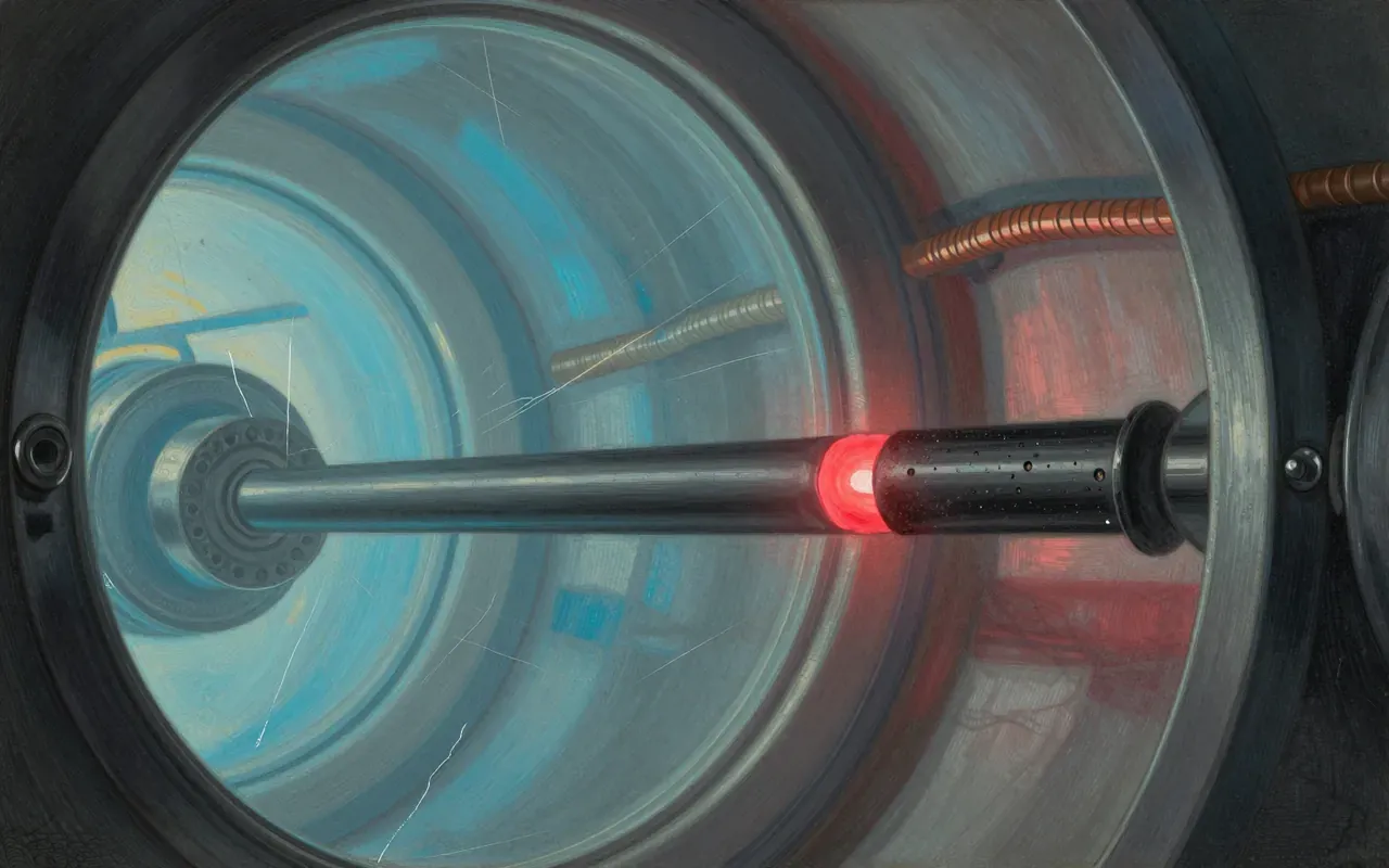
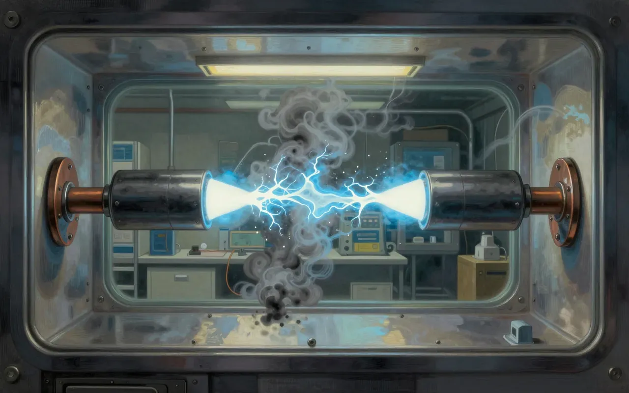
A carbon nanotube is, structurally, a sheet of carbon atoms arranged in the same hexagonal lattice found in graphite, rolled into a seamless cylinder only a few nanometres across, in some cases as narrow as half a nanometre. Sumio Iijima, then working at NEC in Japan, described multi-walled versions of this structure, cylinders nested one inside another, in a 1991 paper examining the soot deposited when an electric arc is struck between two graphite electrodes, a process previously studied mainly for producing fullerenes. His paper generated an unusually large and sustained wave of scientific interest, and it is Iijima’s name that is most closely associated with the discovery of carbon nanotubes as a result, even though he was working from material other researchers had also examined before.
A discovery with a longer history
The historical record complicates any simple story of a single discovery moment. In 1952, Soviet scientists L. V. Radushkevich and V. M. Lukyanovich published images of carbon tubes roughly fifty nanometres across, but the work was largely unnoticed outside the Soviet Union, hampered by the publication barriers of the Cold War period. Morinobu Endo separately observed hollow graphite tubes produced by chemical vapour growth in 1976, and John Abrahamson presented related evidence at a carbon conference in 1979. None of these earlier reports produced anything like the research surge that followed Iijima’s 1991 paper, which suggests that timing and scientific context, rather than the observation itself, largely determined which report became the field’s reference point.
Why 1991 was the moment that stuck
What made 1991 different was less the images themselves than the moment they arrived in: the recent discovery of fullerenes had already convinced much of the materials science and chemistry community that carbon was capable of forming striking, technologically interesting structures beyond graphite and diamond, so a paper describing tubular carbon structures found an audience primed to take it seriously and follow up quickly. Iijima and colleagues went on, in 1993, to develop catalytic methods for producing single-walled carbon nanotubes specifically, a thinner and structurally simpler variant than the multi-walled tubes of his original paper, and that follow-on work helped establish nanotube research as a sustained field rather than a one-off finding, with Iijima receiving major recognition including the Benjamin Franklin Medal and the Kavli Prize in the years since.
Strength well beyond steel
The properties that have kept researchers interested are genuinely striking but come with real limits. Measured tensile strength for multi-walled nanotubes has reached as high as 63 gigapascals in testing, with individual shells estimated near 100 gigapascals, giving carbon nanotubes a strength-to-weight ratio far above high-carbon steel. Their electrical behaviour depends sensitively on the precise geometry of how the hexagonal lattice is rolled into a tube, described by a pair of parameters that determine whether a given nanotube conducts like a metal, with some capable of carrying current densities theoretically thousands of times greater than copper, or behaves instead as a semiconductor. Producing nanotubes with precisely controlled geometry and properties at scale, however, has remained a persistent practical challenge rather than a solved problem.
Metal or semiconductor, depending on geometry
The wider significance of the 1991 paper is that it opened carbon nanotubes as a serious subject of study across electronics, materials science, and medicine, fields that have pursued them for uses including electrical interconnects that could outperform copper, lightweight composite materials that borrow their exceptional strength-to-weight ratio, and biosensors or drug-delivery systems that exploit their small scale and surface chemistry. Three decades of research have produced real advances in each of these directions without yet delivering the kind of ubiquitous commercial deployment that fullerenes’ early hype once suggested, a gap that reflects how much harder manufacturing nanotubes with consistent, controllable properties has proven than simply discovering that the structures exist.
From lab curiosity to material of interest
This is worth the time both for the science and for what it reveals about how discoveries get attributed: the 1952 Soviet images are a useful reminder that being first to observe something is not the same as being credited with discovering it, and that scientific context and timing matter as much as priority. The mechanical and electrical property figures give the story real substance rather than leaving it as an abstract materials curiosity, and readers who follow nanotechnology news will likely recognise how much of the field’s continuing promise traces directly back to this one 1991 paper. Anyone wanting a finished account of nanotubes already transforming everyday products, though, should note that much of the application section remains potential rather than realised.