Seeing single atoms
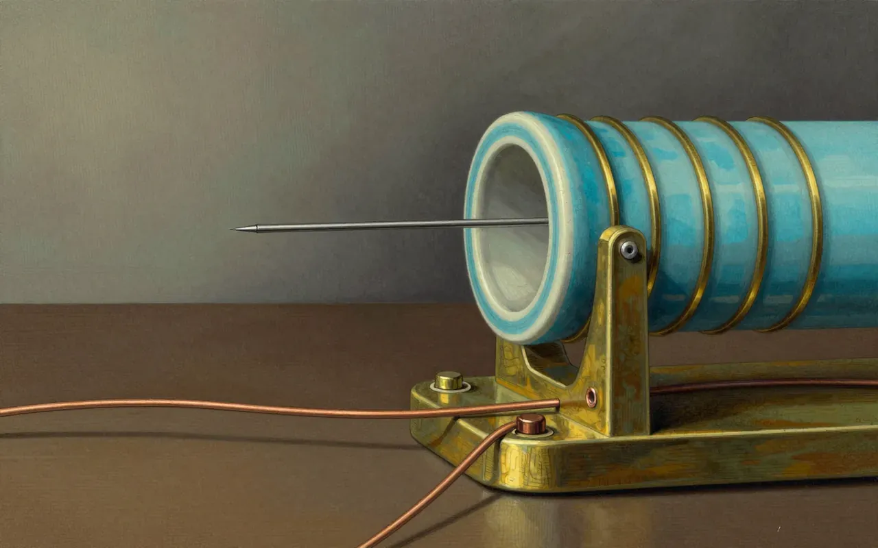
In 1981, working at IBM’s research laboratory in Zurich, Gerd Binnig and Heinrich Rohrer built an instrument capable of resolving surface features smaller than a tenth of a nanometre, with a depth sensitivity down to a hundredth of a nanometre, fine enough to make individual atoms on a surface visible one by one. What they had built was the scanning tunnelling microscope, and it did not rely on light or on any conventional lens; it worked by bringing an extremely sharp conducting tip, typically made of tungsten, platinum-iridium or gold, close enough to a surface that a small applied voltage would drive a measurable current across the gap between them, a gap the tip and surface never actually touch.
A current across a vacuum gap
That current exists because of quantum tunnelling: electrons can cross a vacuum gap they would have no classical means of crossing, and the probability of them doing so falls off extremely quickly as the gap widens, with the tip typically held only four to seven angstroms from the surface. Because the tunnelling current is so sensitive to this distance, and to the local density of electronic states at each point on the surface, moving the tip across the sample while monitoring or holding constant that current traces out a map of the surface at atomic resolution. The physics behind tunnelling itself was well established well before Binnig and Rohrer’s work; what their instrument did was turn that established effect into a usable measurement.
Holding a tip steady to a few atoms’ width
The real achievement, and the one the Nobel committee singled out, was experimental rather than theoretical: getting a tip to hold a position within a few atomic diameters of a surface reliably enough to scan it required piezoelectric scanner tubes capable of extraordinarily fine positioning, along with vibration isolation systems, sometimes magnetic levitation, sometimes carefully tuned mechanical springs, to keep outside disturbances from swamping a signal that small. That combination of components has held up as the working template for the instrument ever since, adapted into variants that now operate in ultra-high vacuum at temperatures near absolute zero, in ordinary air, in liquids, or at temperatures above a thousand degrees Celsius, depending on what is being studied.
What it cannot do
The technique has a firm boundary: it depends on an actual tunnelling current flowing between tip and sample, which means both need to conduct electricity, and it cannot directly image an insulating surface at all. The most detailed, highest-resolution work also generally still needs the isolation of ultra-high vacuum and very low temperatures to suppress the kind of thermal and mechanical noise that would otherwise overwhelm the tiny currents involved. That gap in what the scanning tunnelling microscope could do is part of what pushed Binnig, working with Christoph Gerber and Calvin Quate, to invent a related instrument in 1985, the atomic force microscope, built specifically to extend atomic-scale imaging to insulating materials the original design could not reach.
From imaging to arranging atoms
Once the instrument could resolve individual atoms, it was a short conceptual step to using the same tip to move them, and researchers at IBM demonstrated exactly that by positioning individual xenon atoms on a nickel surface, arranging matter one atom at a time rather than simply observing it. That capability, imaging and manipulation combined in a single instrument, became one of the founding tools of nanotechnology, the deliberate construction and study of structures at the atomic and molecular scale. Related techniques grew directly out of the core method, including scanning tunnelling spectroscopy and spin-polarised variants, each extending what could be measured at a surface beyond a simple topographic map.
A shared Nobel, five years on
This is a story worth knowing because the physics involved, tunnelling across a barrier, was not new when Binnig and Rohrer began; what was new was the patience and engineering needed to make that old effect do useful work at the scale of single atoms. Recognition came quickly by the standards of physics, with Binnig and Rohrer sharing half of the 1986 Nobel Prize in Physics only five years after the instrument’s construction, alongside Ernst Ruska for earlier work on the electron microscope. For anyone interested in how instruments, rather than new theories, can open an entire field, from atomic imaging to the atomic force microscope that followed it, this is a compact and well-documented case.